Silicon metalens selected by Optics & Photonics News as one of the significant progresses in 2018
Source: School of Physics
Written by: School of Physics
Edited by: Wang Dongmei
Metalenses are able to focus light using subwavelength artificial nano-structures. Metalenses made in titanium dioxide, gallium nitride, and silicon nitride have already exhibited impressive optical performance in the visible regime such as lack of spherical aberration and near-unity numerical aperture (NA). When it comes to NA values higher than 1, however, immersion liquids are needed to increase the background refractive index. At this point, metalenses lose their ability to focus light due to the reduced index contrast. A question is: how can metalenses achieve ultra-high NA?
In 2017, we introduced crystalline silicon as a promising material for metalenses, even in the visible regime, and demonstrated high NA and high transmission. We then implemented the geometric phase approach with nanobricks in the arrangement of spherical-aberration-free phase profile and designed a metalens with an NA = 0.98 in air. Due to the high refractive index of the crystalline silicon, this metalens can be further front-immersed into immersion oil to achieve an ultrahigh NA of 1.48 experimentally and 1.73 theoretically on a sapphire substrate, thereby showing the highest numerical aperture in the visible regime ever reported. This work was published in Nano Letters, 18(7), 4460-4466, 2018. It was also selected as one of the most significant optical progresses in 2018 by Optics Society of America and published in Optics & Photonics News. This work was authored by Dr. Haowen Liang, Prof. Jianying Zhou and Prof. Juntao Li from School of Physics at Sun Yat-sen University and corresponding authored by Prof. Juntao Li.
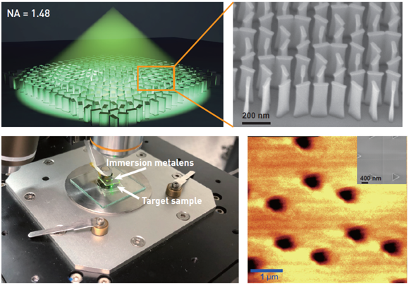
Our work highlights several exciting aspects of metalenses: they can achieve diffraction-limited operation even for an ultrahigh NA of 1.48; they can achieve competitive performance compared to conventional objective lenses in the scanning imaging mode, and they can be made in silicon, so they are readily CMOS compatible. Using a hybrid optimization algorithm for the design with a target function that emphasizes both phase fidelity and high transmission, we have also shown that the best crystalline silicon nanobrick arrangement can reach high transmission values that are comparable to those made in dielectric materials such as titanium dioxide; thus, it validates that sophisticated computational optimization is an effective tool for nano-structure design. We envision that this design will push metasurfaces into practical applications such as high resolution, low-cost confocal microscopy and achromatic lenses.
Link to the paper: https://pubs.acs.org/doi/10.1021/acs.nanolett.8b01570